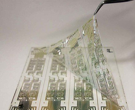
An organic field-effect transistor (OFET) is a field-effect transistor using an organic semiconductor in its channel. OFETs can be prepared either by vacuum evaporation of small molecules, by solution-casting of polymers or small molecules, or by mechanical transfer of a peeled single-crystalline organic layer onto a substrate. These devices have been developed to realize low-cost, large-area electronic products and biodegradable electronics. OFETs have been fabricated with various device geometries. The most commonly used device geometry is bottom gate with top drain and source electrodes, because this geometry is similar to the thin-film silicon transistor (TFT) using thermally grown SiO2 as gate dielectric. Organic polymers, such as poly(methyl-methacrylate) (PMMA), can also be used as dielectric. One of the benefits of OFETs, especially compared with inorganic TFTs, is their unprecedented physical flexibility, which leads to biocompatible applications, for instance in the future health care industry of personalized biomedicines and bioelectronics.
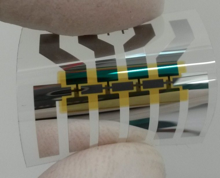
In the field of organic field effect transistors (OFETs), we have demonstrated a simple method, of extended ultraviolet–ozone (UVO) treatment to modify the PDMS surface and effectively employed it in solution-processed OFETs as a gate dielectric material. The modified PDMS surface showed enhanced wettability and adherence to both polar and nonpolar liquids, which is contrary to the generally observed hydrophilic nature of UVO-treated PDMS surfaces because of the creation of polar functional groups. The modified PDMS is then used as a gate dielectric in solution-processed n- and p-channel OFETs using [6,6]-phenyl-C61-butyric acid methyl ester (PC60BM) and regioregular poly(3-hexylthiophene) (rr-P3HT) semiconductors, respectively. Our group has also realized the fabrication of PDMS-based solution-processed OFETs using a liquid crystal (LC), 2-decyl-7-phenyl-benzothienobenzothiophene (Ph-BTBT-10), as a semiconducting channel material, exhibiting high electrical performance such as a high hole mobility of ∼22 cm2 V–1 s–1, a low threshold voltage (<1 V), and a high current on/off ratio of 105. We have also investigated the various factors affecting bias stress and hysteresis behaviour of PDMS based solution-processed OFETs and found that the choice of dielectric, semiconductor materials and different atmospheric conditions significantly affect bias stress and hysteresis .